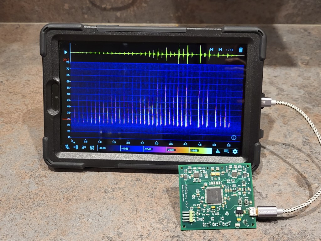
The BatGizmo is a full spectrum bat detector that I started work on during covid lockdown. This page outlines the design decisions that I took, including both the successful and the less successful ones. My hope is that this will prove useful to others.
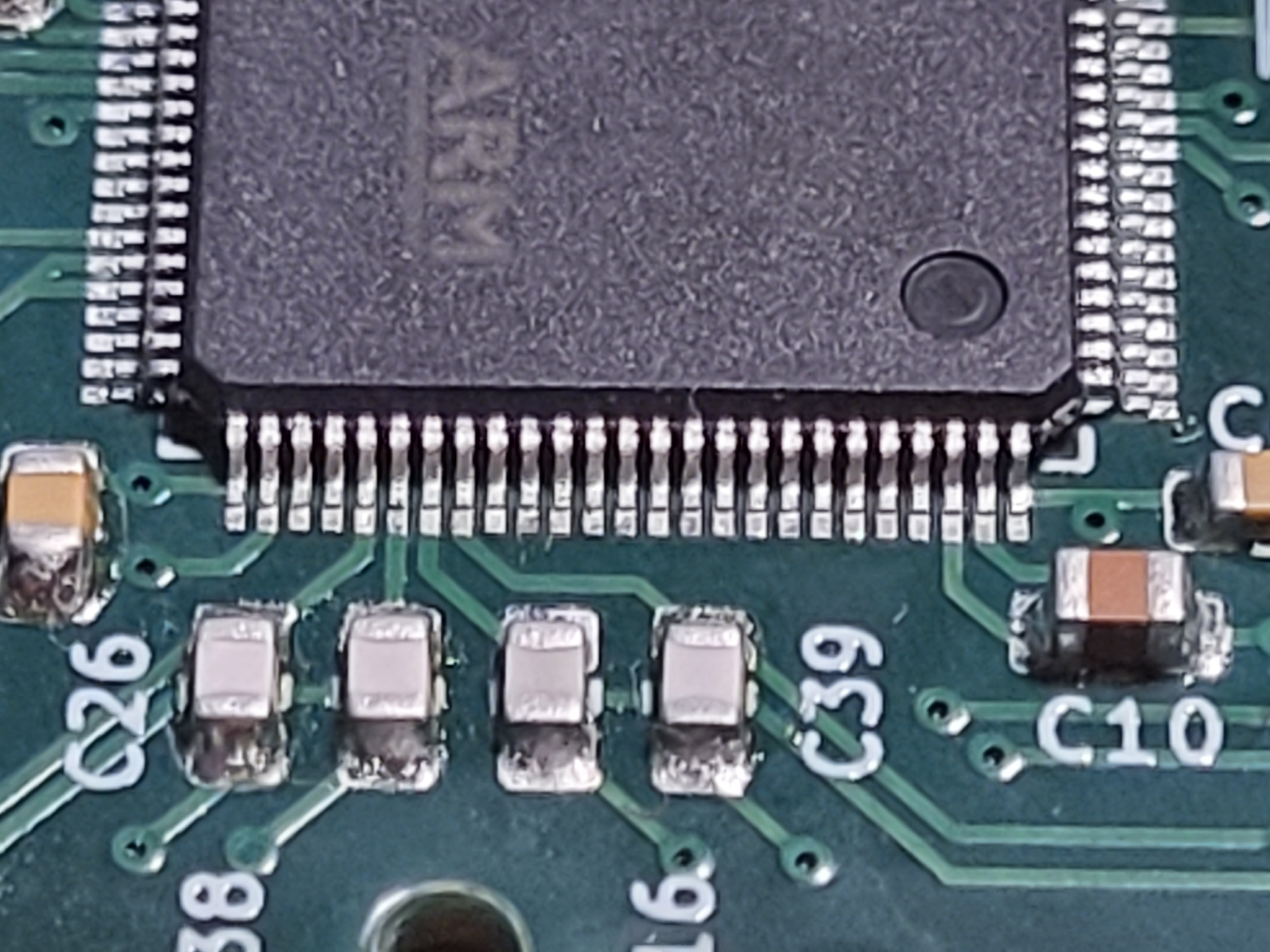
Gallery
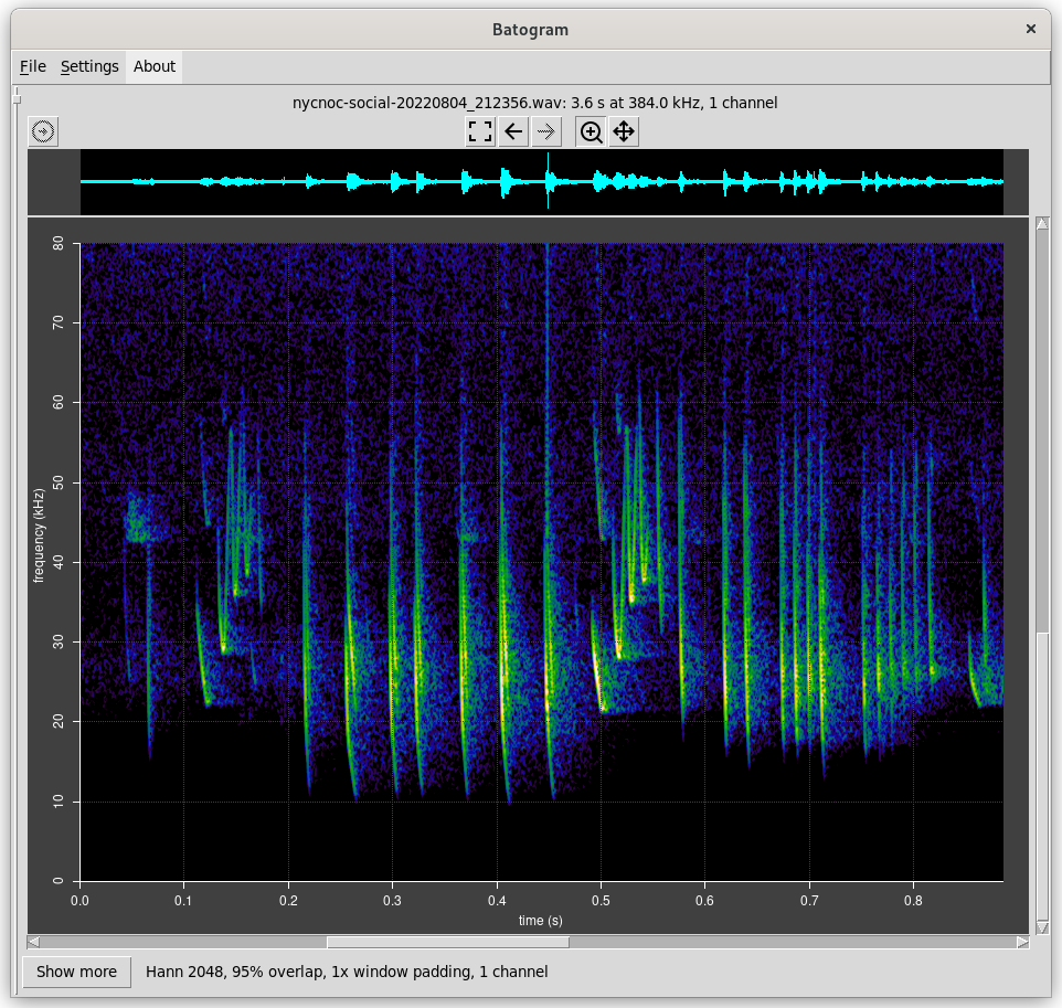
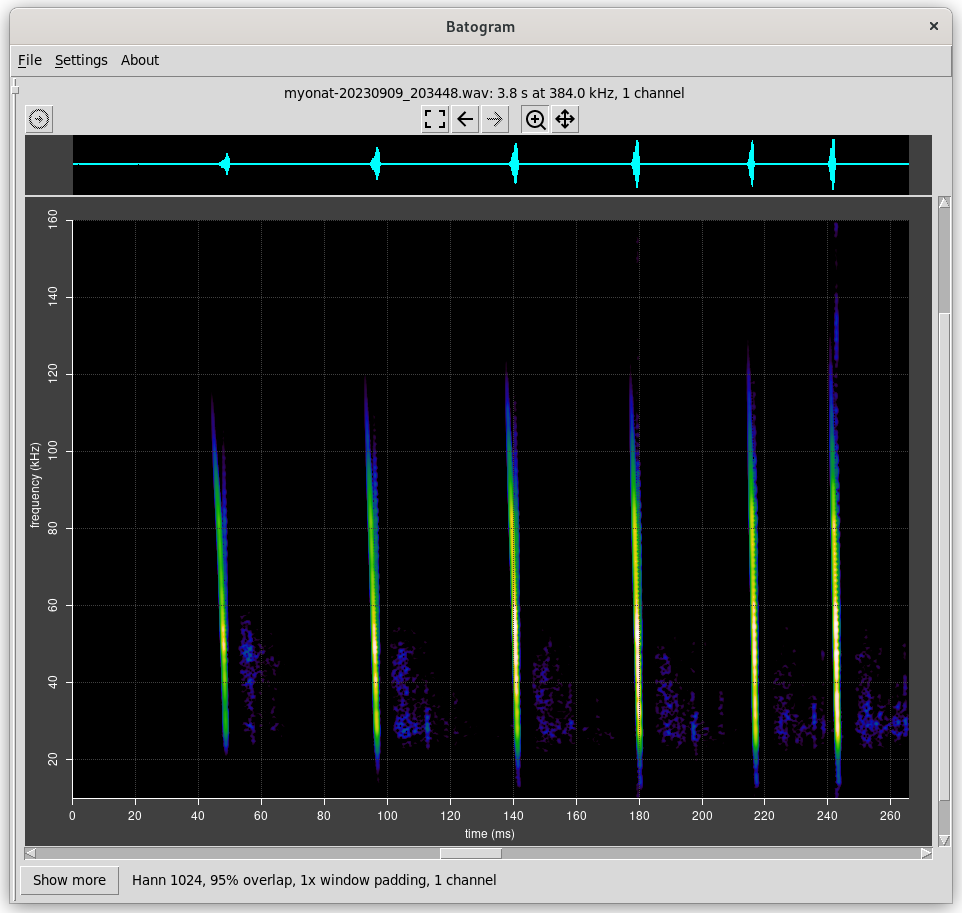
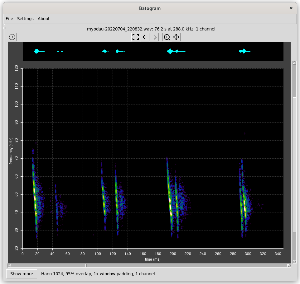
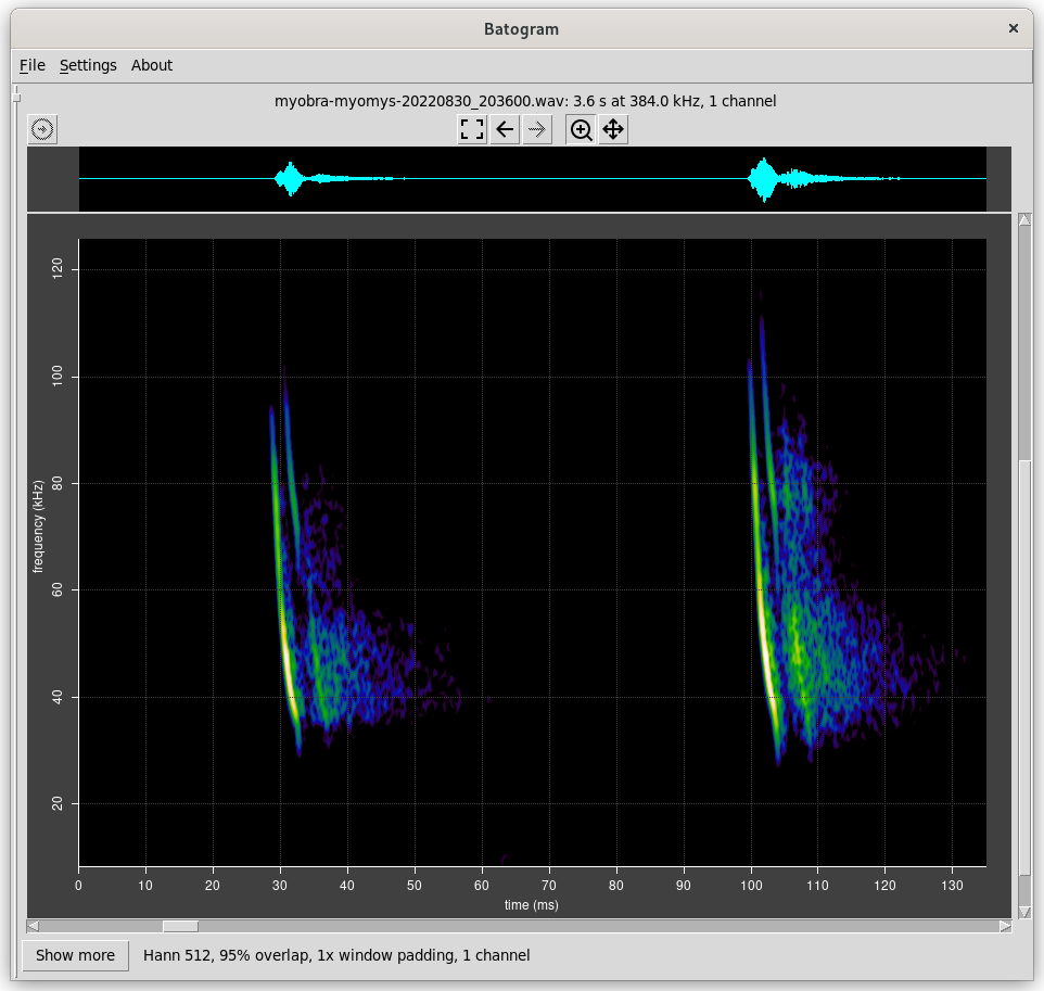
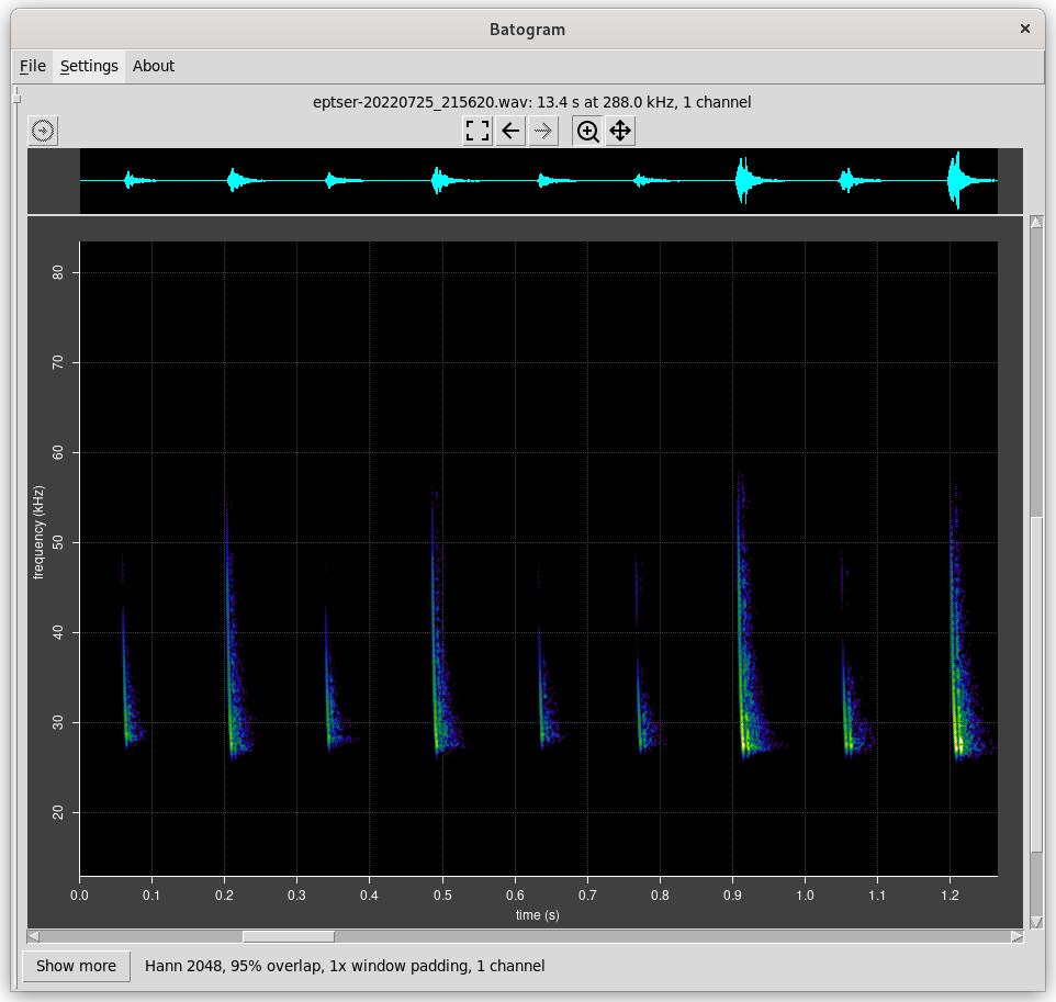
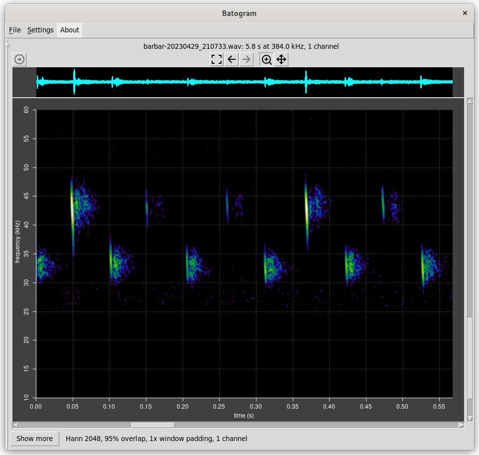
Spectrograms are rendered with batogram.
Aims
My aim was to design and build a detector that I could use on an evening stroll to identify bats that I noticed. The BatGizmo is not intended to be used as an unattended data logger – that would require different design decisions.
There are different kinds of bat detector which require different complexities of circuitry, outlined here.
I decided to build a full spectrum detector. This makes for a somewhat complex electronics, but allows for more accurate bat identification than simpler types. Modern electronics makes the complexity and cost very manageable.
Basic Approach
A full spectrum detector needs various elements to be useful. These include a microphone, obviously, but also some electronics to process the raw signal, and some digital sampling and processing to create a spectrogram. It’s also useful to have some kind of user interface for controlling sensitivity and scaling, and some kind of persistent storage for data.
There are a couple of different basic approaches that can be taken. One is to use a compact single board computer such as a Raspberry Pi, with a display and means of control such as a touch screen or simple keypad. This would result in a small self contained unit that can be easily carried, and can be plugged into a computer network to transfer recorded data as required.
Another approach is to make use of the fact that almost everyone carries a phone in their pocket, which provides a user interface, storage and plenty of processing power. Android phones usually include a USB connector that allows an ultrasonic microphone to be plugged in. Android itself is a fairly open platform well supported with software development tools. In fact, an excellent app for visualising bat spectrograms already exists.
In general I have taken the view that electronics is cheap, and tended to over engineer rather than under engineer. The complexity and cost of this design could certainly be reduced somewhat.
The Design
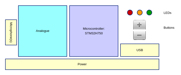
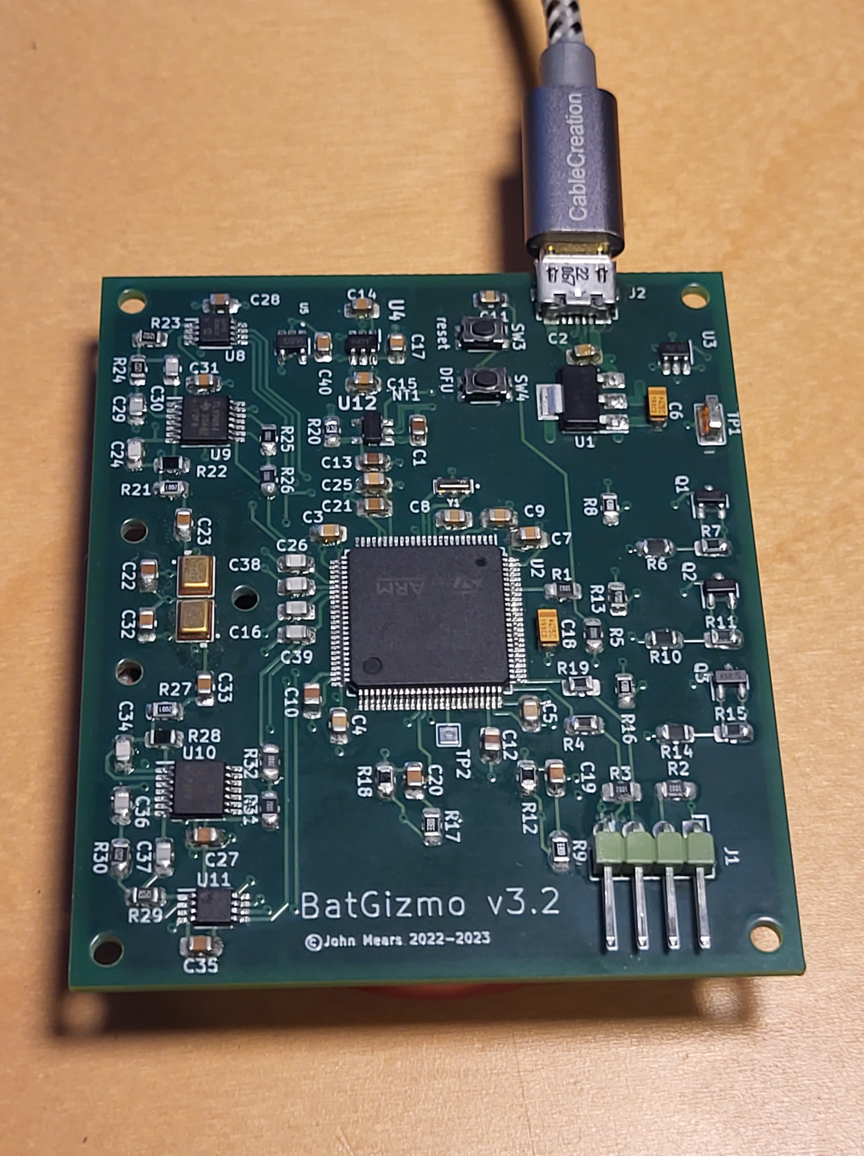
The BatGizmo design consists of the following major components:
- Two microphones, to allow for stereo recording and experimentation with beam forming techniques.
- Analogue electronics to condition the raw signal.
- A microcontroller (MCU), which samples and converts the analogue signal to digital form, does some digital signal processing, and makes the result available via USB.
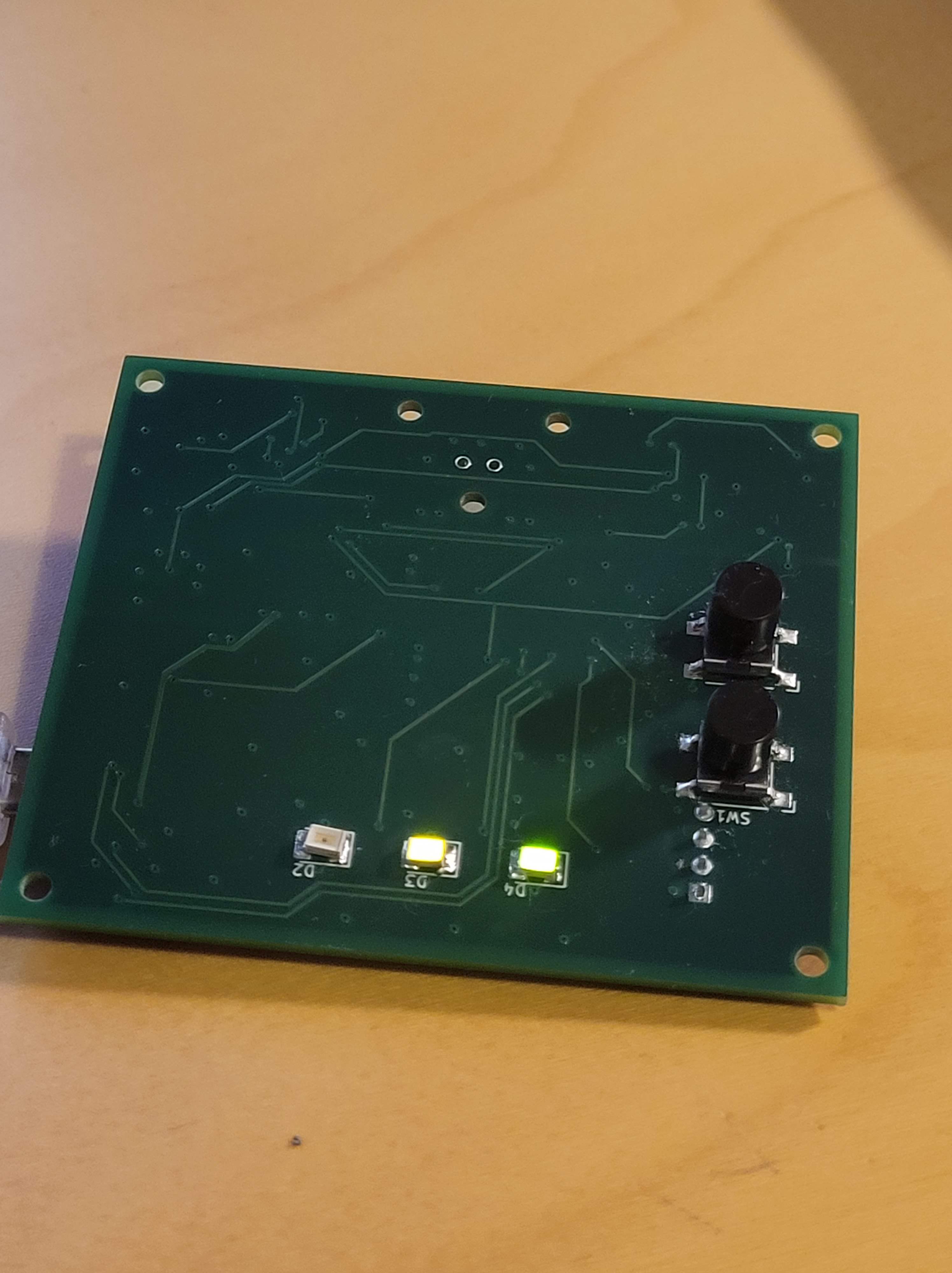
- Some LEDs which provide various indications under microcontroller control (overload, USB connection, USB synchronized).
- An up and down button, which allow the gain to be chosen.
- A USB master device, not shown, which might be a phone, a tablet or a computer, which processes and displays the audio in the form of a spectrogram.
These components are discussed in more detail below.
Signal Path
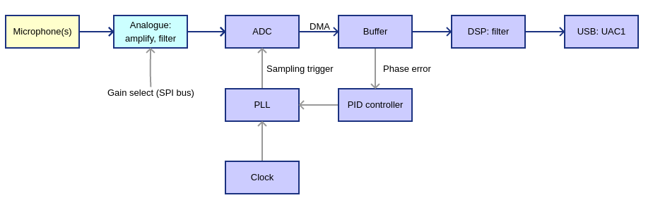
The microphone I used includes a signal preamplifier and produces an analogue output. The signal is further amplified and filtered in preparation for sampling by the analogue to digital converter (ADC) in the microcontroller. The MCU sets the gain via an SPI (serial parallel interface) bus, to both audio channels in parallel, in response to presses of the up and down buttons.
The MCU contains three high quality analogue to digital convertors. These sample and convert the analogue signals to 16 bit digital values. The sampling rate has to match the rate at which the USB host requires data, to avoid artifacts in the signal. This is somewhat complex and is described below in more detail.
Sampled data is written into a circular buffer by DMA, which transfers 1 ms frames of data. Data frames are then copied into processing buffers for digital signal processing, and finally into a USB buffer for transmission to the connected USB host.
Component Detail
The Microcontroller
The microcontroller (MCU) is the heart of this design. Many kinds of MCU are available with widely varying specifications, costs and maturity of support. I had previously experimented with a few MCUs, and come to the conclusion that the most important criterion was to choose one with mature support. In my view that boils down to:
- Excellent documentation.
- Mature development tools and libraries, preferably open source.
- An online community of developers.
In other words, a mature ecosystem. That points towards an ARM processor of some kind. Some more specific technical requirements are:
- Inclusion of a high resolution and high speed ADC.
- Good USB support.
- Flexible clocking.
- Basic digital I/O, SPI and other standard buses
- Lots of processing power to allow for experimentation with digital signal processing.
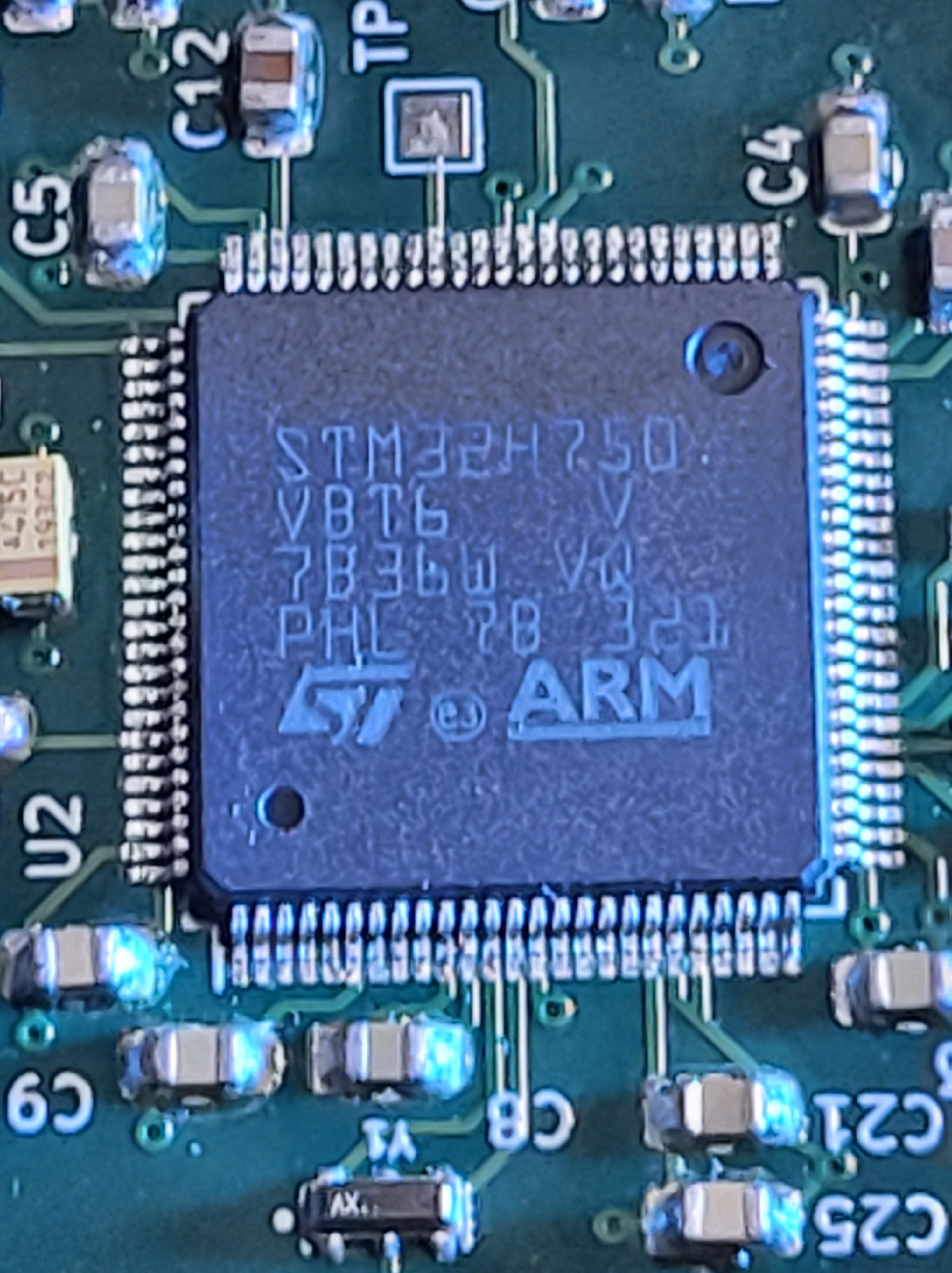
I settled on the STM32H7xx family of processors. These are very mainstream and mature with a strong ecosystem, both commercial and hobbyist. The STM32H750 is billed as the “value line” version of STM’s highest spec MCU, at the time time of writing, and costs around £12 in one off quantities.
Development tools include STM32CubeIDE, which is an interactive IDE for C and C++ programming based on the open source gcc compiler. It has support for interactive debugging, the CMSIS library, which includes DSP functions optimized for ARM. It can also automatically generate code for more many common use cases – really useful for a chip as complex as this.
This choice of MCU proved to be a good one. One could argue that it is over specced. I think this is not a bad thing for an experimental project of this kind. I did experience some supply chain challenges including long lead times during the covid crisis. Supply seems to be back to normal as of mid 2023, with chips available from mainstream suppliers once again.
The STM32H7xx family of MCUs is documented here. More details on the STM32H750 are here. Development boards and debugging probes are available from aliexpress at low cost, and from mainstream suppliers at moderate cost.
MCU Support Circuitry
This application note is an introduction to hardware development for STM32H7xx, including an example circuit which is easily adapted. It includes advice on PCB layout. This was the starting point for my design.
Power supply for the MCU is derived from the USB host, and is described in more detail below.
A number of decoupling capacitors and some other passive components are prescribed by the application note. These must be fitted as close to the MCU possible.
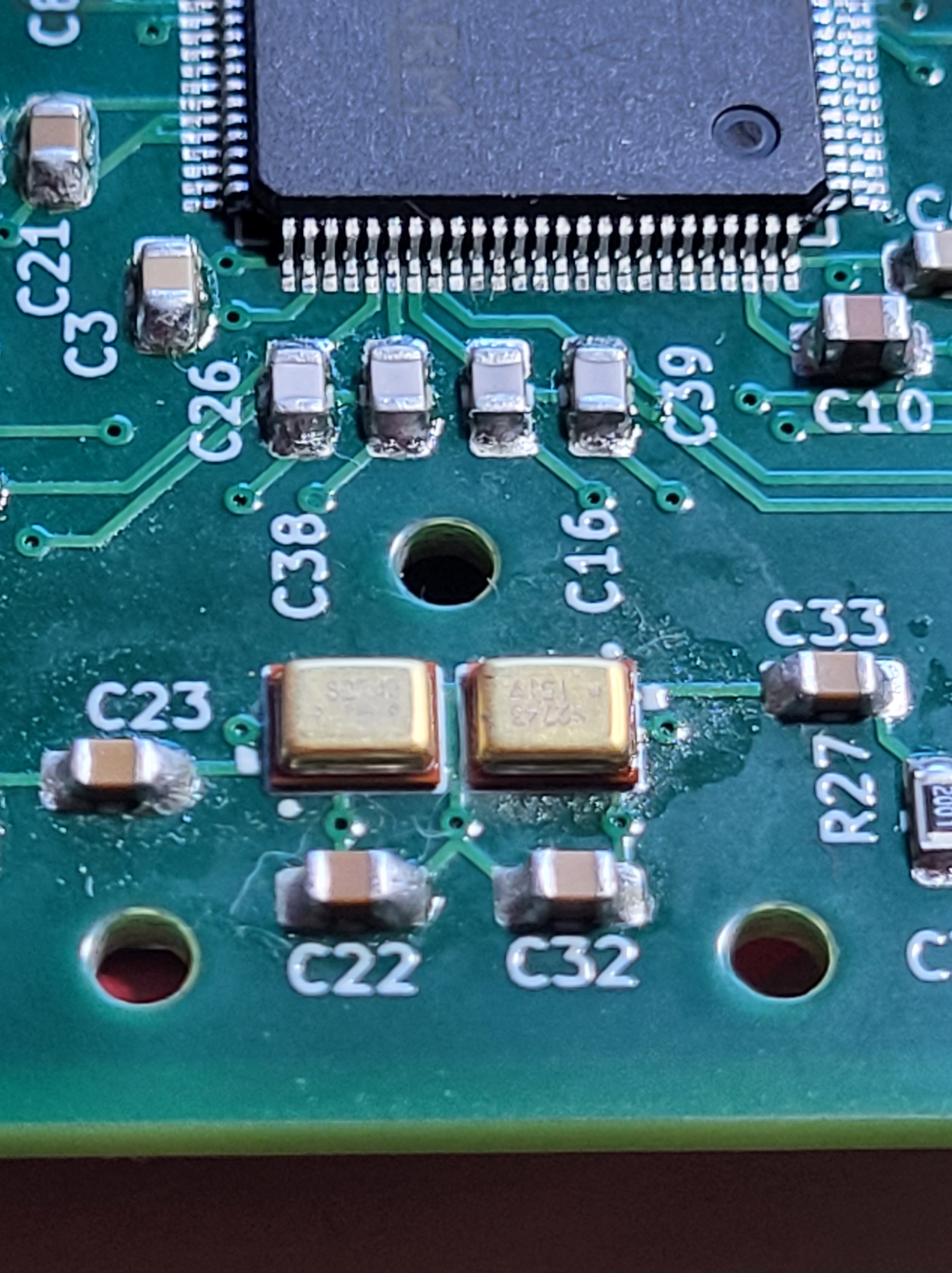
The STM32H750 has various options for clocking, including an internal high speed RC clock. This is attractive to remove the need for an external crystal. However, the internal clock proved not to be sufficiently stable, so I settled on an external 16 Mhz ceramic resonator. This only adds one to the component count, and is tiny.
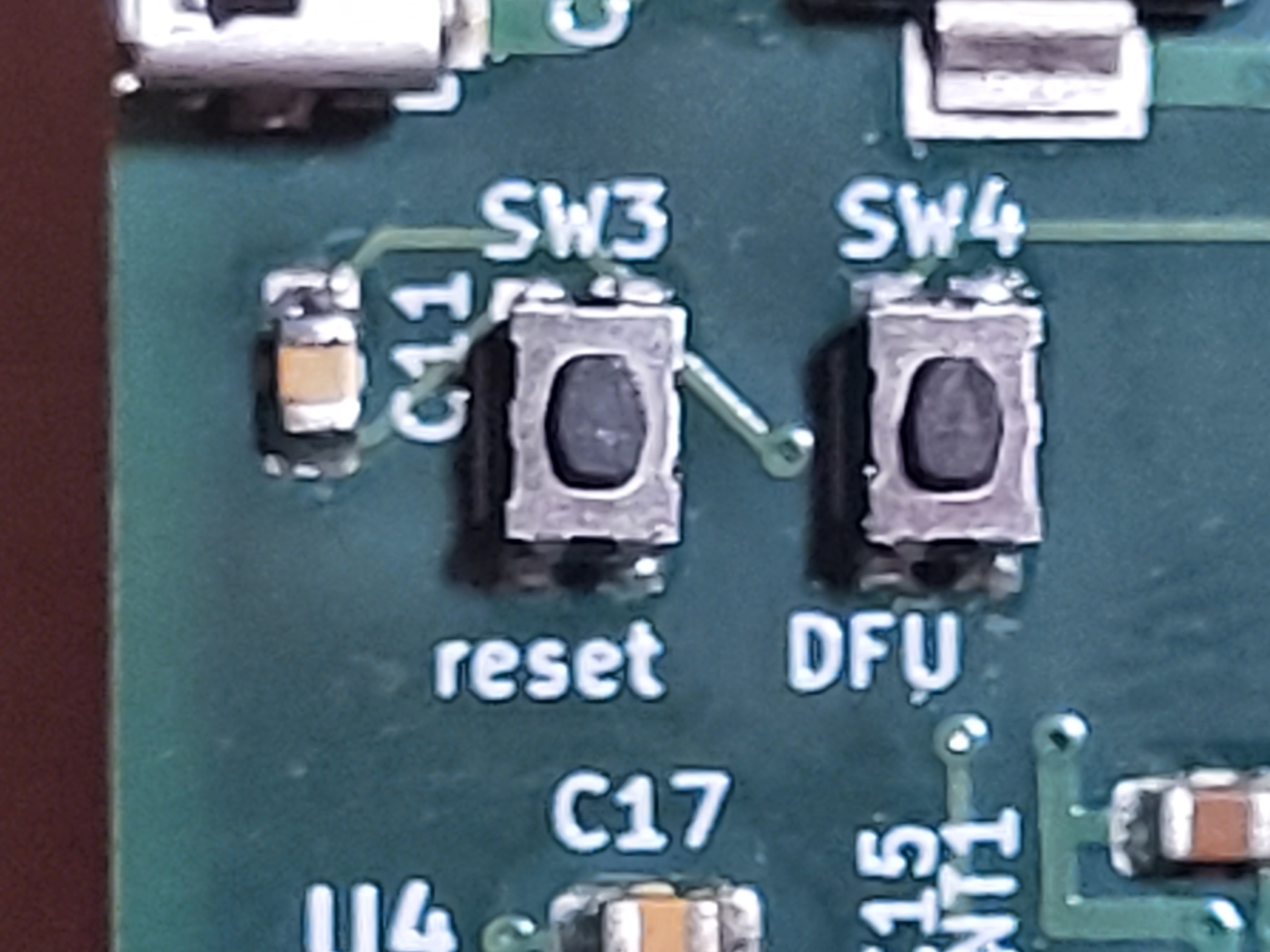
The MCU includes boot loader firmware which can be used to upload firmware to flash storage via various protocols, including USB Direct Firmware Update (DFU). This is convenient as free DFU clients are available for major computing platforms (linux, Windows, MacOS). Two micro switches are included in this design for this purpose, “reset” and “DFU”, connected respectively to NRST, and BOOT0 on the chip. DFU mode is entered by holding the DFU button down while clicking the reset button. At this point, the MCU present itself as DFU device:
[jmears@semele ~]$ lsusb -d 0483:df11
Bus 001 Device 015: ID 0483:df11 STMicroelectronics STM Device in DFU Mode
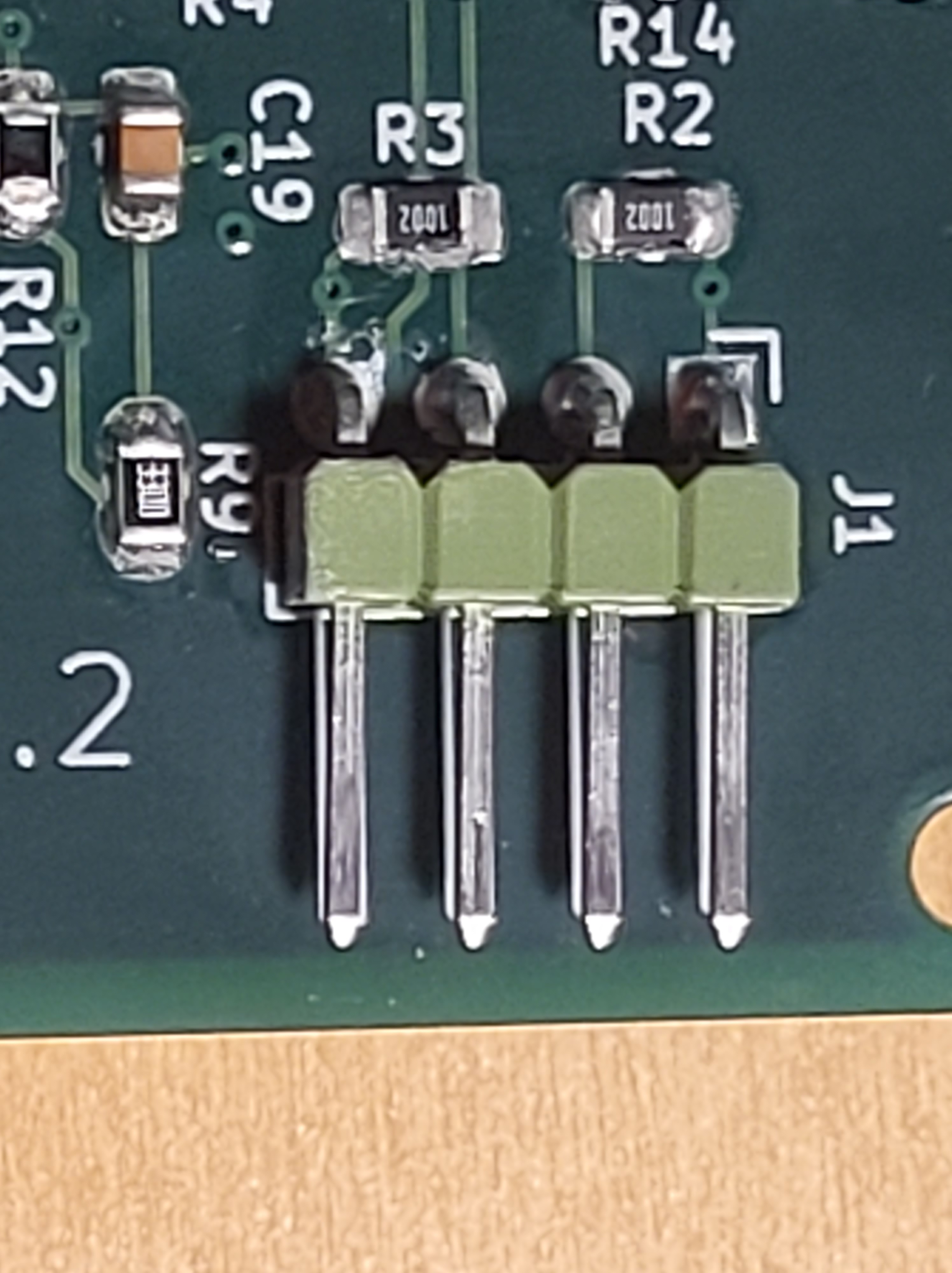
The MCU supports interactive debugging, and firmware update, via a Serial Wire Debug (SWD) interface. I chose the four pin version of this interface which was entirely sufficient. It is connected to a four pin PCB connector (J1) which need only be populated if interactive debugging is required. SWD is a high speed interface, so 22 ohm terminating resistors are included in the SWD clock and data lines to minimise ringing.
In addition, some digital IOs are wired to drive LEDs and detect the state of the up and down buttons.
The Microphones
The BatGizmo design includes two microphones, to allow for stereo recording and experimentation with beam forming.
There is an interesting published review of various microphones for wildlife applications here. Sadly, the review fails to reach any clear conclusions for ultrasonic applications.
Generally, microphone manufacturers don’t publish much about microphone responses in the ultrasound range. An exception is Knowles, who publish limited data suggesting that the SPU0410LR5H-QB MEMS microphone has sensitivity up to at least 80 kHz. This microphone has an analogue output, so some external analogue amplification, filtering andADC circuitry is needed. Knowles also make similar microphones with a built in sigma-delta ADC, which eliminates the need for external circuitry or ADCs. However, this approach limits flexibility. Typically, sigma delta ADCs employ noise shaping which concentrates noise at higher frequencies, in the region of interest for detecting bats.
I chose the SPU0410LR5H-QB analogue microphone. Although external analogue circuitry is required, it offers most flexibility and avoids the problem of noise being concentrated in the region where microphone sensitivity drops off. They are available at low cost from mainstream electronics supplies – between 50p and £1 per microphone, depending on quantity. They can also be obtained presoldered onto a PCB for easy experimentation.
Knowles offer a wide range of MEMS microphones, including some that allow gain control from an external voltage. These would be worth investigating – I didn’t do that.
I soldered the microphones directly to the PCB, each with a 1mm hole through the PCB, aligned with microphone ports. I also provided three other holes in the PCB to allow an acoustic horn to be located and secured.
In retrospect, I am happy with the choice of microphone, and the trade for flexibility versus additional external circuitry. Electronics is cheap. I have had clear bat detections at frequencies up to around 150 kHz, which the range required for native British bats.
For completeness, it is worth noting some down sides of the SPU0410LR5H-QB:
- Its output is analogue, so you need some external analogue circuitry, with care over grounding and power supply to avoid noise and interference.
- Its sound port is open, so any water or dirt that gets in will most likely degrade or destroy the microphone. However, they are cheap, and replacement is feasible with the right tools.
- Their frequency response is not flat – I guess that the internal chamber has a resonance. However, this is easily corrected during data analysis.
- Hand soldering is tricky – but possible. I describe one method here. Other methods are possible, such as use of solder paste and heat from a hot air soldering gun.
Analogue Processing
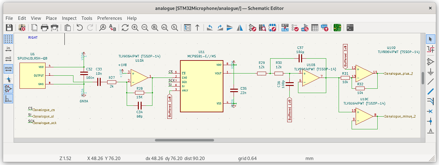
Analogue processing uses standard amplification and filtering stages. All analogue components are powered from a dedicated analogue 3.3V supply, and a 1.8V voltage reference is used for level shifting. The op amp chosen has a nominal gain-bandwidth product of 10 MHz, chosen to comfortably exceed the bandwidth required for bats. It describes itself as low noise. More on that later.
Throughout, chip power supplies are decoupled according to the manufacturers’ application notes.
The microphone output signal is high pass filtered with C33/R27 which provides a zero at about 8 kHz. This blocks DC and reduces unwanted audio below the range of bats.
An inverting amplifier (U10A) provides a gain of 7.5, and a zero which rolls off gain at 6 dB per octave above 156 kHz. This is to eliminate unwanted ringing from the amplifier, and contribute to anti-alias filtering (more below). It also provides level shifting to 1.8V. Note that any noise or inteference present in the 1.8V reference is amplified with the full gain used for the signal, so needs to be very clean. More on this later.
U11 is a programmable gain amplifier. Its bandwidth comfortably exceeds the range needed for bats. Its gain can be selected from one of 1, 2, 4, 5, 8, 10, 16 or 32 from the MCU, via an SPI bus. This is an intrusion of digital signals into the analogue domain – but the SPI bus is inactive almost all the time, and so avoids introducing unwanted digital signal.
U10B is configured as a Sallen-Key filter – low pass with two zeros at 133 kHz, Q=0.5. This provides a level of anti-alias filtering, together the single zero from U10A, making a total of 18 dB per octave drop in gain above 156 kHz.
Finally, a pair of inverting and non inverting buffer amplifiers drive the differential inputs to the MCU ADCs. These are high bandwidth amplifiers to be able to maintain their output in the presence of an extremely short current pulse into the ADCs sampling circuitry. Use of a differential input to the ADCs results in a higher effective number of bits (more on this below).
Not shown in this circuit diagram is a 47 pF capacitor from each analogue line to ground very close to the MCU. This provides a low impedance source of charge for the ADC sampling circuit.
Usual PCB layout precautions are taken in respect of the analogue circuitry: separation from the digital circuitry, and a dedicated analogue ground plane.
Aliases and Anti-alias Filtering
Anti-alias filtering is required in sampling systems to reduce artefacts that result when a sampled signal contains components above the Nyquist frequency. When sampling at 384 kHz, the Nyquist frequency is 192 kHz. Any signal above 192 kHz appears as a reflection below 192 kHz, which is an undesirable artefact.
In applications such as high quality audio reproduction, aliasing introduces distortion and is highly undesirable. Consequently, these systems use high order filters reduce aliasing to a very low level. These filters are complex.
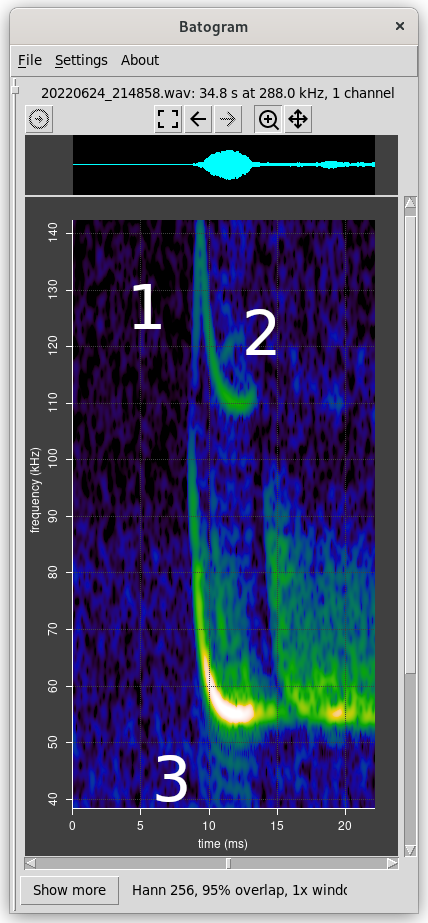
In bat related applications, this is much less critical. There is very unlikely to be any natural sound above 192 kHz in the UK, though a low level of microphone self noise may be present. If any component of a bat call is above 192 kHz, it will appear inverted below 192 kHz when viewed in a spectrogram. This is obvious to the eye and easily ignored.
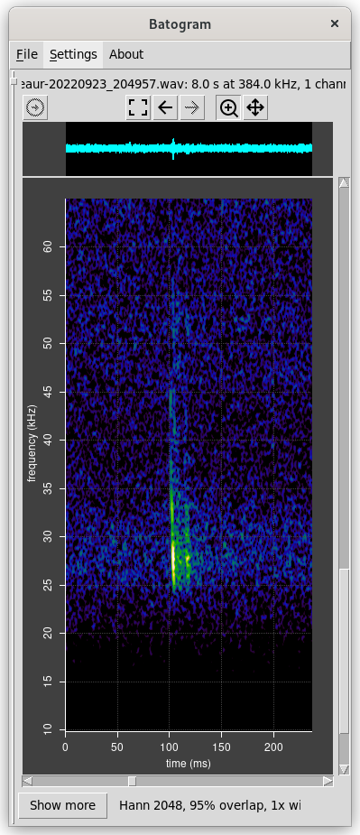
As an example, imagine that a 110 kHz rhinolophus hipposideros echolocation call is being sampled at 384 kHz. The Nyquist frequency is 192 kHz. For a natural sound or microphone noise to alias to 110 kHz, it would need to be at 274 kHz. In very round numbers this is one octave above the third order zero provided by filter, so is attenuated by 18 dB.
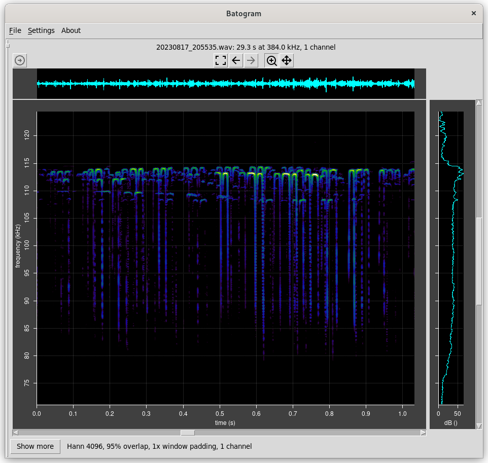
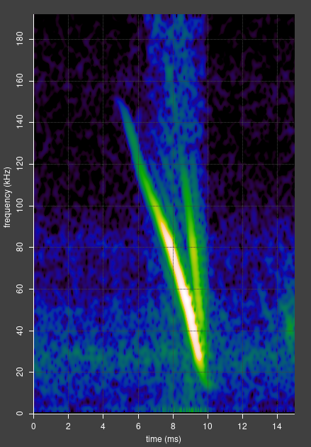
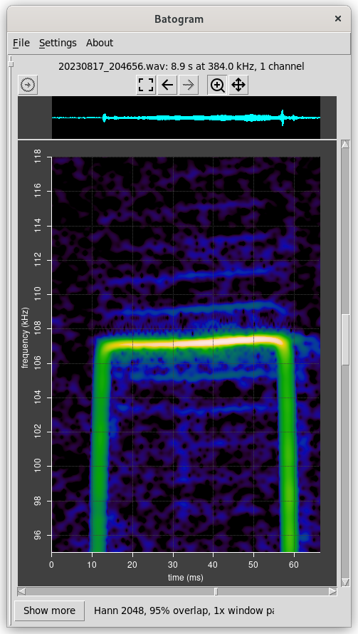
The discussion above applies only to signals originating from before analogue filtering. High frequency components can also be introduced after filtering, for example, as a result of non linearities in analogue or digital processing. In that case, they are not attenuated by the anti-alias filtering, and may be visible. See the example on the left, where non-linearities in the ADC result in artificial harmonics, parts of which are aliased in the Nyquist frequency (144 kHz in this case).
Analogue to Digital Conversion
One of the strengths of the STM32H7xx series of MCUs is the presence of three high quality built-in analogue to digital converters (ADCs). Two of them are used in this design. They are 16 bit successive approximation (SA) converters which can be kernel clocked at a high rate – resulting in sampling rates up to 3.6 Msps each. This means that audio data can be sampled at a rate of 384 kHz in each channel, while still allowing for a level of oversampling to reduce noise.
There are excellent application notes on getting the best out of the STM32H7xx ADCs here and here. This design adopts the recommendations from these documents to achieve best accuracy and resolution.
According to the application notes linked above, the highest effective number of bits (ENOB) that can be obtained from these ADCs is 13.7. That is obtained by using differential analogue inputs. An ENOB of 13.7 means that the two and a bit least significant bits (LSBs) are noise. However, even the noise bits have some value as they can be averaged via oversampling to obtain more precision. Rounding the ENOB to 14 for simplicity, the maximum dynamic range that can be achieved is about 84 dB. That number will give us a comparison when we consider self noise and interference levels.
Audio CDs are sampled at 44.1 kHz and have 16 bit resolution, providing a dynamic range of about 96 dB, for comparison.
A known challenge with SA ADC converters is their reliance on the accuracy of capacitor values used in their internal switched ladder networks. Highly accurate capacitors are hard to manufacture. Inaccuracies result in non linearity in conversion. In turn, non linearity results in artificial harmonics which are visible in spectrograms. Luckily, there is a solution to this. The ADCs in the STM32H7xx series MCUs include a self calibration routine, which can be run as often as required under control of the firmware. The application note recommends to re-run the calibration when the temperature changes significantly. In this design, the firmware runs self calibration on startup and reset.
I did a simple sanity test to assess the ADC linearity, after self calibration. I configured an ADC to take its input from the on chip 12 bit DAC. This was driven by firmware to generate a mathematically calculated sine wave, sampled by the ADC, and processed into a spectrogram in the same way as a real signal. A faint artificial second harmonic was visible, approximately 70 dB beneath the fundamental. The theoretical best dynamic range from the 12 bit DAC is 72 dB. This is only semi scientific test, but gives some confidence that the ADCs are accurate to at least this level.
There is another challenge with ADCs in the STM32H7xx, relating to timing. Signal sampling and conversion is timed based on the the kernel clock provided to the ADC. However, sampling is triggered at a variable rate designed to synchronise with the host’s USB frame rate. These two clock frequencies are inevitably not exact multiples. Any difference results in a variable latency between each trigger and the actual sampling and conversion. The latency is a function of the difference in frequency between the sampling rate and (a fraction of) the kernel clock rate. As one clock gradually drifts relative to the other, the trigger latency gradually changes, until one clock overtakes the other, at which point the latency resets. The result is a slow periodic timing error which can be considered as multiplying the signal with a complex saw tooth. Multiplying two periodic functions with harmonics results in a set of sums and differences, which are visible as a set of faint side bands in the spectrogram. Fortunately there is a solution – the ADC kernel clock frequency must be controlled to track an exact multiple of the sampling rate.
Power Supply, Broadband Noise and Interference
Bat calls are often extremely loud. However, there are also situations where they can be extremely quiet. For example:
- An evolutionary arms race between long eared bats and their prey has resulted in them having extremely quiet echolocation calls.
- For similar reasons, barbastella barbastellus feeding buzzes are very quiet.
- High frequency calls from bats such as lesser horseshoes attenuate rapidly over distance, so they can be very quiet when they reach the microphone.
To be able to detect quiet calls, unwanted signals need to be minimised. Microphone self noise is outside the control of this design, as are acoustic echos from the environment, and not considered here. However, broadband noise and interference can arise from other sources within the detector, and externally from its USB host, and need to be carefully minimised.
Specific sources of noise include:
- The external USB power. The detector derives all its power from the host’s USB 5V line. This frequently contains lots of unwanted components, such as 1 kHz and its harmonics (the full speed USB frame rate), components from switch mode power supplies which may run at ultrasonic frequencies, and other digital sources in the host device.
- The MCU in the detector drives the USB bus to transmit data back to the host. This requires significant current to be drawn from its power supply, introducing 1 kHz and its harmonics into the power supply.
- Broadband noise originating from basic physics in the power regulators and voltage reference within the detector.
The points of greatest sensitivity to unwanted electrical signals are:
- The microphone itself, via its power supply.
- The first stage of amplification, and in particular the 1.8 V voltage reference used for level shifting, and via its power supply.
To come up with a design that avoids introducing unwanted signals, we have to consider the Power Supply Rejection Ration (PSRR), which quantifies how good a component is at preventing unwanted signal from its power supply being added to its output. For simplicity I will consider 50 kHz as the frequency of interest in the context of bats. Usually, both the PSRR and level of noise drop off with frequency.
Here are some numbers for comparison in what follows:
- The maximum precision of our 14 bit ADC is 84 dB.
- At the maximum detector gain setting:
- Total detector gain is about 8 x 32;
- The 14 bit LSB on the differential 3.3V ADC inputs is equivalent to 0.4 mV;
- That is equivalent to 1.6 uV raw microphone signal.
The general strategy for power supply involves four chips, as follows:
- The raw USB 5V input powers two independent 3.3V regulators in parallel. One generates digital power (VDD) and one generates analogue power (VDDA). This isolates digital noise originating from the MCU from the analogue circuitry.
- Digital and analogue circuitry is located in different regions on the PCB, with separate ground planes; power traces to the two are separate.
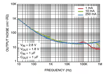
- The VDDA regulator (NCV8163) is intended for high bandwidth (RF) applications and describes itself as low noise, high PSRR. Its PSRR is 85dB at 10 kHz, dropping to 60 dB at 100 kHz.
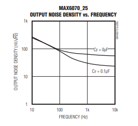
- The 1.8 V reference is generated by a dedicated voltage reference (MAX6070AAUT18+T). Its PSRR is around 50 dB at 50 kHz.
Consider the microphone. Normal precautions have been taken in PCB layout so the main source of unwanted signal is likely to be via its power supply. Sadly, Knowles don’t publish a PSRR, but their design guide alludes to 60 dB, which we have to assume is at audio frequencies – it will be less at ultrasonic frequencies. We’ll pessimistically assume 30 dB. The PSRR of the analogue regulator adds a further 60 dB (pessimistically), totalling 90 dB. 100 mV variation on the raw USB power would result in 3 uV, a little more than our 1.6 uV comparison above. Remember, these calculations are pessimistic is is probably fine.
Regulator noise at the microphone power supply will be attenuated by the microphone PSRR. The NCV8163 data sheet gives a noise density of about 20 nV per root Hz at 50 Khz; assuming FFT buckets of 1 kHz width, this comes to about 0.6 uV. That compares favourably with our 1.6 uV comparison above, even without the microphone PSRR.
Now consider the 1.8 V reference used to level shift the signal. This is a direct input to the first amplification stage – any unwanted signal must therefore be less than 1.6 uV. Unwanted signal from the raw USB power input is attenuated by first the analogue regulator (PSRR 60 dB pessimistically), then the voltage reference, which adds a further 50 dB. 100 mV variation on the raw USB power would result in 0.3 uV unwanted signal, which compares well with 1.6 uV comparison above.
The MAX6070 data sheet gives a noise density of about 20 nV per root Hz at 50 Khz; assuming FFT buckets of 1 kHz width, this comes to about 0.6 uV. That compares favourably with our 1.6 uV comparison above.
The conclusion of all of this is that while the power supply and voltage reference circuitry may seem over engineered, it is not over engineered by much. Experience (aka mistakes) with earlier versions of this design confirm this.
USB Audio
USB is very complex. I’m not going to attempt to describe it all here, instead, I’ll just outline the basics of USB audio.
USB consists of a host with one or more devices plugged into it. Most commonly, the host is a computer and the devices are things like a keyboard, a mouse, a camera, a speaker, a microphone and so on. The host initiates all transactions, nothing happens on the USB bus without the host initiating it.
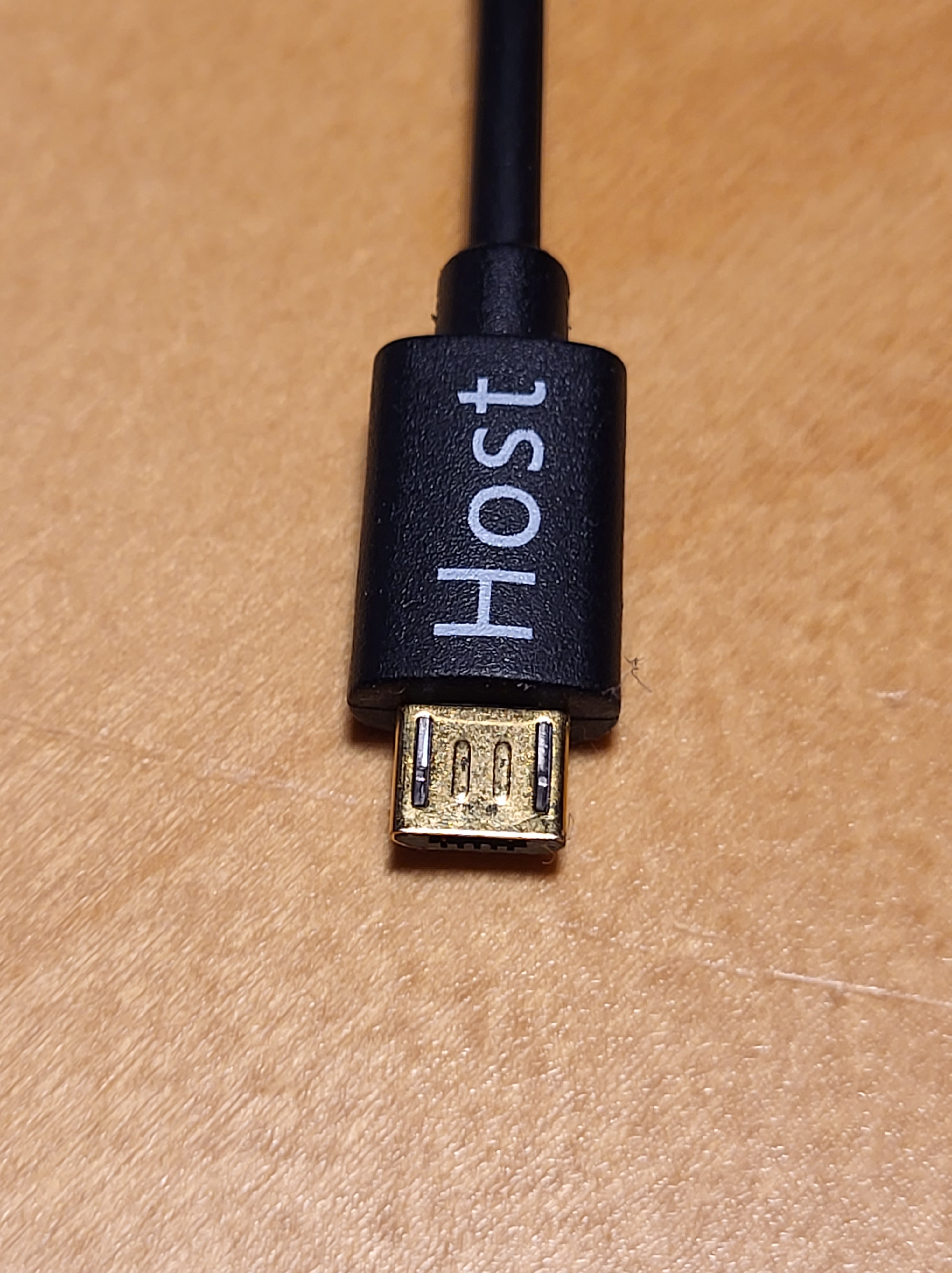
Some devices can act as either a host or device. For example, a phone or tablet can be a storage device (so you can access your photos from your computer), or a sound logger with a USB microphone plugged into it. The type of cable plugged into the phone determines whether it is to act as a host or device. The cable that makes the phone is known as a USB On-The-Go cable. One end is marked “host”; that end must be plugged into the phone.
Data is transferred in frames, whose size and rate depends on the type of device in question and the version of USB being used. In full speed USB (used by this device), the frame rate is one per millisecond. Each audio frame can contain up to 1023 bytes.
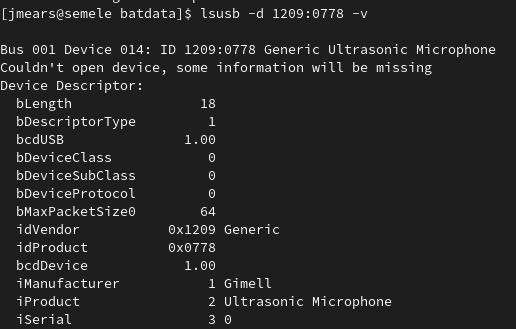
Each device provides a manifest to the host on request, so that the host can discover what endpoints the device has. Endpoints include audio sources such as microphones. You can view the manifest by plugging a device into a computer and typing a suitable command, such as lsusb -d <deviceid> -v on linux. The manifest includes the manufacturer name, the product name, the USB version, the type (microphone), and a list of interfaces and endpoints. The complete manifest is rather long. Full speed USB is used by this design, the fastest that can be supported by the MCU without any additional components.
The manifest for BatGizmo describes an audio endpoint which is an input (relative to the USB host) for audio sampled at 384 kHz with a bit resolution of 16. The transfer type is isochronous and the sync type is none. Isochronous data transfer is intended for streaming video and audio data. The sync type of none indicates that adaptive data rate synchronising will be performed by the device (the microphone), that is, the device will tune its own sampling rate to match the rate expected by the host. This is achieved using auto phase adjustment, described in the next section.
USB is extremely complex to implement. There are libraries to help, but it is still a complex business. I used the TinyUSB library in the BatGizmo because it is widely used and well proven. It includes an implementation of USB Audio Class 2 (UAC2). There are three USB audio classes, of which the first (UAC1) has most widespread support, and is therefore the one used by this device. I achieved this by adapting the AUC2 implementation provided with TinyUSB. The different audio classes are, naturally, incompatible.
I have encountered many protocols in my career. I think USB is one of the worst. It shows every sign of having been designed by a committee, every member of which seems to have insisted that their favourite feature be included.
Here is a reference to USB UAC1. Good Luck.
Data Processing Pipeline
Data is handled in frames for convenience efficiency. A frame corresponds to the data required by a USB audio frame, which is the number of samples corresponding to the 1 ms USB frame rate: 384 in this design. There are separate, parallel frames for each audio channel.
The source of raw data is the ADCs. These sample the microphone signals at a rate determined by their trigger, and the data is written into memory by direct memory access (DMA). The DMA controller generates interrupts when the DMA buffer is half full, and also when it is full. This allows the DMA interrupt handler to be copying one half of the DMA buffer to the circular buffer while the other half is being populated. Use of an intermediate circular buffer allows the ADC frame rate to deviate slightly from the USB frame rate, which inevitably it will.
The STM32H7xx architecture provides different classes of memory. One class is data tightly coupled memory (DTCM), which can be accessed by the CPU within a single instruction cycle. DTCM is the most efficient place to do data processing, but unfortunately it cannot be accessed by peripheral DMA or the USB controller, which limited to slower general purpose memory. DTCM memory used for all internal processing buffers.
The USB controller generates a start of frame interrupt, which triggers the flow of data from the circular buffers through the DSP buffers, to the USB buffer. This interrupt is also used to drive phase locking (see below), it is it given highest priority to minimise interrupt latency and variability.
Digital signal processing is used implement a high pass filter based on 8 kHz, to remove DC signal and uninteresting audio signal without significantly attenuating the low end of myotis bat calls. Further DSP can be performed here, CPU capacity permitting. The final DSP stage copies the data into the USB buffer ready for transmission to the USB host.
Auto Phase Control
As mentioned in the section on USB, the USB frame rate is determined by the USB host, and the USB device (the BatGizmo) has to supply full data frames at that rate. Inevitably, the host clock will differ slightly from the BatGizmo clock, resulting from time to time in either too many or too few data samples being available to populate the USB buffer.
There are different possible approaches to dealing with this:
- Samples may be duplicated or dropped as required to keep in sync. This is conceptually simple; however, this results in visible artefacts in the spectrogram.
- Samples may be resampled at the rate the host requires. However, this is complex and very CPU intensive, and limited to rational ratios.
- Auto phase control: the BatGizmo sampling rate can be adjusted in real time to match the rate required by the host. This is somewhat complex conceptually, but adds very little CPU load, and works well.
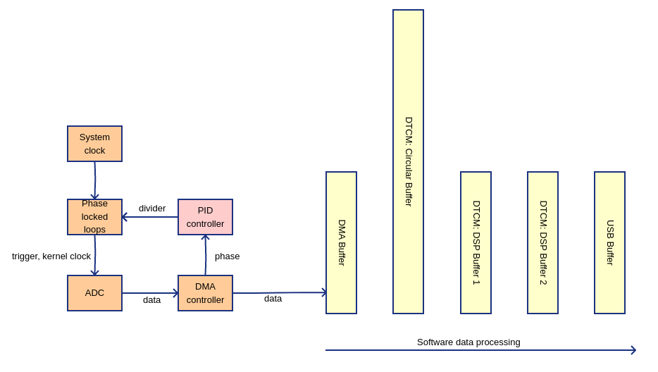
The final method is used by the BatGizmo: auto phase control. This works as follows:
- The USB start of frame interrupt handler (highest interrupt priority) reads the DMA counter from the DMA controller. This value provides a measure of how far through the frame the DMA control has reached at the time of the USB start of frame, effectively indicating the phase of the DMA frame.
- That phase is compared with a target phase that we are aiming to maintaining. In the BatGizmo this is three quarters of the way through DMA frame, chosen so that the USB interrupt and DMA interrupt don’t conflict.
- That phase error from the target is used as the input to a software PID controller.
- The PID controller output drives the clock scaling ratio of a phase locked loop (PLL) within the MCU, varying the rate at which the ADC is triggered so that the DMA phase is maintained very close to its desired value.
In other words, the ADC trigger rate is varied in real time so that on average, the BatGizmo frame rate exactly matches that of the USB host. On a short time scale there will be small frame timing deviations, but these can be absorbed by the circular buffer. In practice, the frame rates match within one sample, so this is very effective. When the phase is locked to a close margin, a green LED is lit.
A nice feature of the STM32H7xx MCU is its flexible PLLs. These support fractional division, allowing the ADC clock rate to be very finely adjusted. In my implementation, the ADC trigger clock granularity is 122 Hz. This is invisible on typical spectrogram scales, even when zoomed in.
As mentioned in the section on the ADC, care has to be taken to avoid varying ADC trigger latency. Failure to do this results in side band artefacts. A constant trigger latency is achieved by driving the ADC kernel clock from a second, parallel, PLL configured to generate an exact multiple of the ADC sampling rate.
Construction
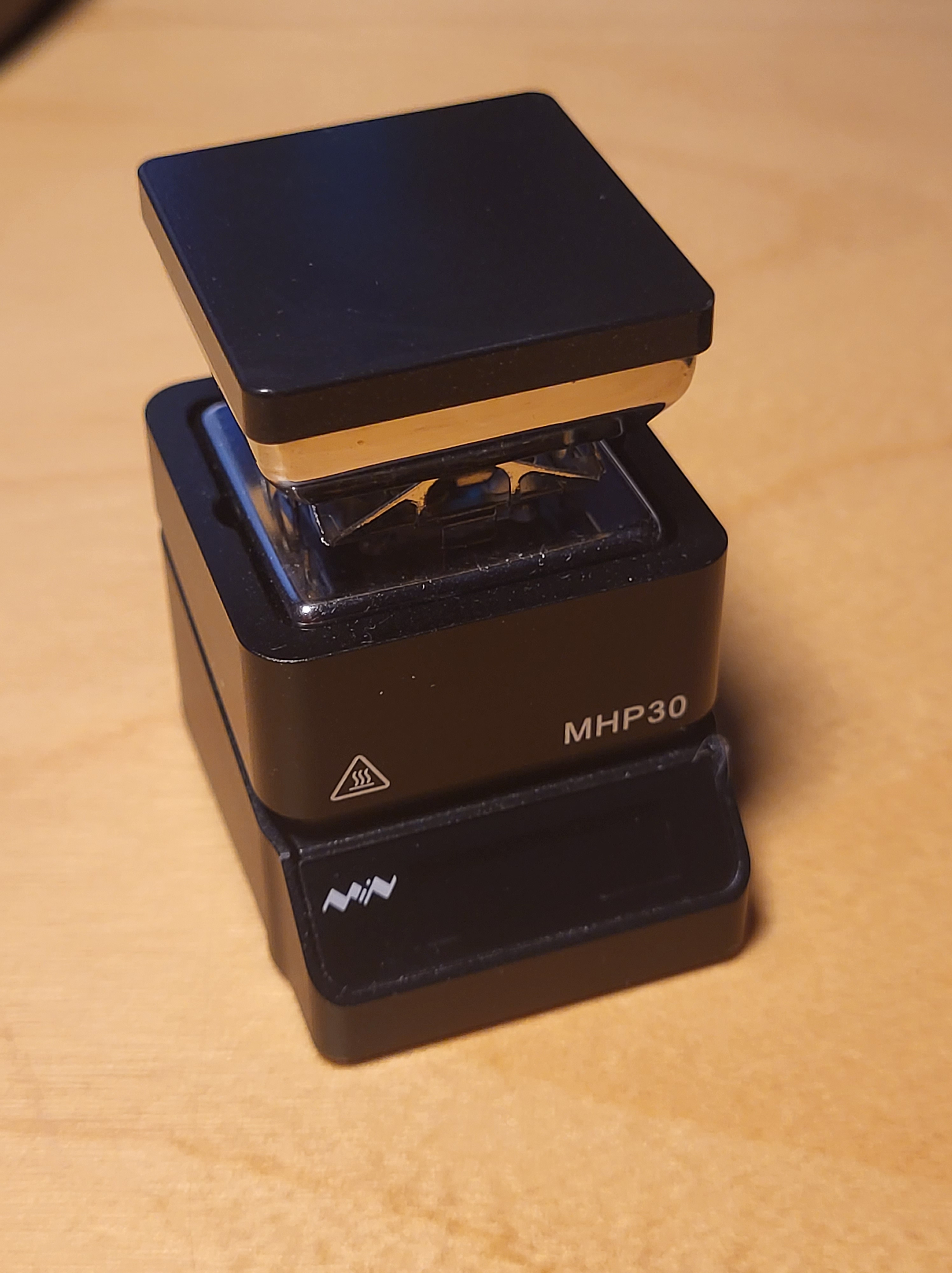
The BatGizmo is constructed using surface mount components. These are intended to be soldered by machine, but with care and practice can be soldered by hand. Generally I used 0805 sized passive components, the largest surface mount size available.
Use binocular magnifiers. Cheap Chinese ones from the internet are fine.
It’s a good plan to practise with sacrificial components first.
Have the PCB tinned with leaded solder, which flows more easily than lead free.
Inspect joints by zooming in with the camera on your mobile phone. It is easy to see which pins have not cleanly reflowed. In that case, add flux and try again.
Pay attention to the temperature of the iron, air and preheater. Leaded solder needs a lower temperature than lead free. Hotter solder flows more easily. MEMS microphones can be damaged by excess heat. Check data sheets for details of maximum temperatures.
Use lots of flux. And even more flux.
The ground plane in a four layer board can conduct heat away from the thing you are trying to solder very effectively. In that case, you probably need to use a preheater under the PCB and hot air from the top at the same time.
I used the following techniques:
- Dab solder paste (a mixture of solder powder and flux) onto each pad on the PCB, and carefully place the component. The paste will hold it in place while you place some more. Several nearby components soldered at the same time in this way. Direct a hot air gun to heat them until the paste turns into molten solder, which will pull the component into alignment. This works well for 0805 passives and larger components. You may need to also preheat the PCB from underneath with preheater set to 270 C.
- Alternatively, tin the pads and contacts on the component with leaded solder, with the iron temperature set to 230 C. Position the component, then use hot air and possibly a preheater from underneath to reflow the solder. This works well for the microphones, though I am told the solder paste method also works well. This method worked well for the USB connector.
- The MCU requires a special technique. It has 100 pins, at 0.5 mm pitch. This needs care and practise. My method was to not add any solder – instead add ample flux and apply a hot 1 mm chisel bit soldering iron (350 C) to pairs of pins. This will reflow the solder from the PCB pads over the pins. Solder diagonally opposite corners first, than stop and review the alignment. If all is good, apply yet more flux and repeat for all the other pairs of pins. The key is no solder, lots of flux, a hot iron.
You can clean off excess flux from the PCB afterwards with a solvent such as isopropyl alcohol. However, don’t let solvent get near the microphones, as it can easily flow into their ports. For this reason, I soldered the microphones last, having cleaned the rest of the board.

2 responses to “BatGizmo – A Full Spectrum Bat Detector”
[…] wrote up my bat detector design, the BatGizmo, in a previous blog. I noted there that it has two microphones and two independent signal processing channels. This […]
[…] A USB microphone of my own design and construction that I could plug into an Android tablet for live detection and recording. […]